- 您现在的位置:买卖IC网 > Sheet目录366 > TMDXEVM5515 (Texas Instruments)EVAL MODULE DSP FOR C55XX
�� ���
���
���SPRS645F� –� AUGUST� 2010� –� REVISED� OCTOBER� 2013�
�3.5�
�3.5.1�
�Configurations� at� Reset�
�Some� device� configurations� are� determined� at� reset.� The� following� subsections� give� more� details.�
�Device� and� Peripheral� Configurations� at� Device� Reset�
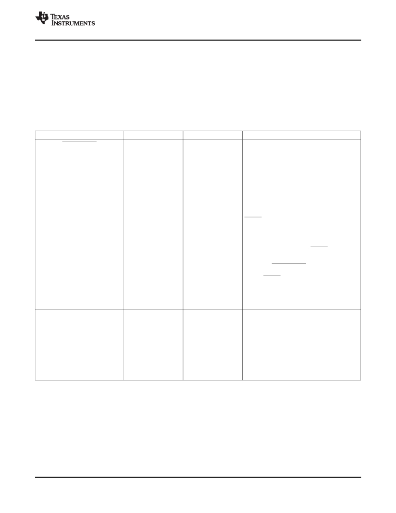
�Table� 3-4� summarizes� the� device� boot� and� configuration� pins� that� are� required� to� be� statically� tied� high,�
�tied� low,� or� left� unconnected� during� device� operation.� For� proper� device� operation,� a� device� reset� should�
�be� initiated� after� changing� any� of� these� pin� functions.�
�Table� 3-4.� Default� Functions� Affected� by� Device� Configuration� Pins�
�CONFIGURATION� PINS�
�DSP_LDO_EN�
�SIGNAL� NO.�
�D12�
�IPU/IPD�
�–�
�FUNCTIONAL� DESCRIPTION�
�DSP_LDO� enable� input.�
�This� signal� is� not� intended� to� be� dynamically�
�switched.�
�0� =� DSP_LDO� is� enabled.� The� internal� DSP� LDO�
�is� enabled� to� regulate� power� on� the� DSP_LDOO�
�pin� at� either� 1.3� V� or� 1.05� V� according� to� the�
�LDO_DSP_V� bit� in� the� LDOCNTL� register,� see�
��monitors� the� DSP_LDOO� pin� voltage� and�
�generates� the� internal� POWERGOOD� signal�
�when� the� DSP_LDO� voltage� is� above� a� minimum�
�threshold� voltage.� The� internal� device� reset� is�
�generated� by� the� AND� of� POWERGOOD� and� the�
�RESET� pin.�
�1� =� DSP_LDO� is� disabled� and� the� DSP_LDOO�
�pin� is� in� high-impedance� (Hi-Z).� The� internal�
�voltage� monitoring� on� the� DSP_LDOO� is�
�bypassed� and� the� internal� POWERGOOD� signal�
�is� immediately� set� high.� The� RESET� pin� (D6)� will�
�act� as� the� sole� reset� source� for� the� device.� If� an�
�external� power� supply� is� used� to� provide� power� to�
�CV� DD� ,� then� DSP_LDO_EN� should� be� tied� to�
�LDOI,� DSP_LDOO� should� be� left� unconnected,�
�and� the� RESET� pin� must� be� asserted�
�appropriately� for� device� initialization� after�
�powerup.�
�Note:� to� pullup� this� pin,� connect� it� to� the� same�
�supply� as� LDOI� pins.�
�CLK_SEL�
�C7�
�–�
�Clock� input� select.�
�0� =� 32-KHz� on-chip� oscillator� drives� the� RTC�
�timer� and� the� system� clock� generator.� CLKIN� is�
�ignored.�
�1� =� CLKIN� drives� the� system� clock� generator� and�
�the� 32-KHz� on-chip� oscillator� drives� only� the� RTC�
�timer.�
�This� pin� is� not� allowed� to� change� during� device�
�operation;� it� must� be� tied� to� DV� DDIO� or� GND� at�
�the� board.�
�For� proper� device� operation,� external� pullup/pulldown� resistors� may� be� required� on� these� device�
�configuration� pins.� For� discussion� on� situations� where� external� pullup/pulldown� resistors� are� required,� see�
��This� device� also� has� RESERVED� pins� that� need� to� be� configured� correctly� for� proper� device� operation�
�(statically� tied� high,� tied� low,� or� left� unconnected� at� all� times).� For� more� details� on� these� pins,� see� Table� 2-�
��Copyright� ?� 2010–2013,� Texas� Instruments� Incorporated�
��Product� Folder� Links:� TMS320C5515�
�Device� Configuration�
�57�
�发布紧急采购,3分钟左右您将得到回复。
相关PDF资料
TMDXEXP1808L
KIT EXPERIMENTER FOR AM180X
TO263-3EV-VREG
BOARD EVAL TO220-3/TO263-3 VREG
TO263-5EV-VREG
EVAL BOARD VREG TO220-5/TO263-5
TOOLSTICK-EK
KIT TOOL EVAL SYS IN A USB STICK
TPS23757EVM
EVALUATION MODULE FOR TPS23757
TPS62230EVM-370
EVAL MODULE FOR TPS62230-370
TRAVELCUBE
SURGE SUP 1OUT W/RJ11 DIRECTPLUG
TRAVELER100BT
SURGE SUP 2OUT W/RJ11 DIRECTPLUG
相关代理商/技术参数
TMDXEVM5515
制造商:Texas Instruments 功能描述:TMS320C5515 DSP Evaluation Module
TMDXEVM642
制造商:Texas Instruments 功能描述:Tools Development kit For Use
TMDXEVM6424
功能描述:开发板和工具包 - TMS320 C6424 DSP Eval Mod RoHS:否 制造商:Texas Instruments 产品:Experimenter Kits 工具用于评估:F2802x 核心:TMS320 接口类型:UART, USB 工作电源电压:
TMDXEVM6446
制造商:Rochester Electronics LLC 功能描述:DAVINCI EVM BUNDLE W/O EMULATOR - Bulk 制造商:Texas Instruments 功能描述:DAVINCI EVM BUNDLE W/O EMULATOR - Bulk
TMDXEVM6446T
制造商:Texas Instruments 功能描述:DM6446 DIGITAL VIDEO EVALUATION MODULE - Boxed Product (Development Kits)
TMDXEVM6446TS
制造商:Texas Instruments 功能描述:DM6446 DIGITAL VIDEO EVALUATION MODULE - Trays
TMDXEVM6452
功能描述:开发板和工具包 - TMS320 C6452 EVM Evaluation Module RoHS:否 制造商:Texas Instruments 产品:Experimenter Kits 工具用于评估:F2802x 核心:TMS320 接口类型:UART, USB 工作电源电压:
TMDXEVM6455
功能描述:开发板和工具包 - TMS320 C6455 Evaluation Module RoHS:否 制造商:Texas Instruments 产品:Experimenter Kits 工具用于评估:F2802x 核心:TMS320 接口类型:UART, USB 工作电源电压: